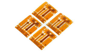
Designing Circuits for Flexible PCBs
A flex circuit board can cut a product’s weight significantly while providing the performance and reliability of a rigid PCB. However, re-designing a traditional circuit to work on a flex PCB can pose unique challenges. The main challenge is to balance the electrical requirements with the mechanical demands of a thin and flexible board that will stand up to vibration, shock, and other environmental stresses.
A PCB designer’s typical tolerance capabilities are not necessarily matched to the realities of the manufacturing process for a flex circuit. Tolerances must be balanced against other design factors such as etching and plating parameters, copper thicknesses, and line properties. The result is that it can be challenging to achieve an acceptable level of impedance (which is measured in ohms) for a signal or power path in a flex board.
Rigid and flexible pcb board are manufactured from a variety of materials. The choice of material will have a big impact on the cost and reliability of the finished product. The thermal expansion of the different materials is also important to consider, particularly when transitioning from rigid sections to a flexible section.

Challenges of Designing Circuits for Flexible PCBs
The flexibility of a flex circuit means that the distance between a hole or via (plated or un-plated) and a copper trace may change over time. This can affect the quality of the finish and cause failures in the product. It is crucial to ensure that there is a sufficient distance between drill to copper on a flex circuit, and it is often easier to achieve this with the use of microvias compared to traditional via holes.
When designing a multi-layer flex PCB, it is important to stagger the locations of the signal traces. This is to prevent the copper from being fatigued over a period of time. The staggering of traces is especially critical when the board is going to be bent, as the bending causes stress on the copper.
Many times designers are guilty of adding complex features to their flex PCB designs that do not add any value to the final assembly. This can be the case with features such as blind and buried vias, or layers of solder mask. While these features are necessary in some applications, it is important for a designer to keep in mind that the more layers and complexity of a flex PCB the higher the cost will be.
It is also a good idea to talk with your supplier about their capabilities and recommendations when designing for a flex circuit board. They will have experience and insight that can help you avoid some common pitfalls. They can also provide you with a quote for the production of your flex PCB. By taking the time to do this, you can ensure that your flex circuit board will be fabricated without any unnecessary issues that can drive costs up or cause delays in the delivery of your completed product.
