
Design-For-Manufacturability in Rigid Flex Circuit Designs
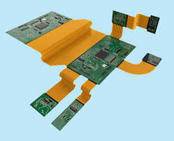
Rigid flex circuits are used in a wide variety of electronic and industrial applications. They provide space-saving solutions that are ideal for space-constrained products such as wearable electronics and mobile devices. Rigid flex circuits combine the best of rigid and flexible PCB technologies, but they can still be challenging to design. The challenges can range from determining impedance requirements and maintaining these values throughout the stack-up, preserving bend cycle and radii to managing trace routing and component placements. The design team must also consider thermal expansion and moisture absorption during assembly and operation.
Fortunately, there are ways to minimize these design-for-manufacturability (DFM) issues for rigid flex PCBs, and a solid understanding of flex/rigid-flex processing and manufacturing can help. During the design phase, it is important to understand these process capabilities so that designers can make informed decisions about the material selection and layout of the PCB. This will ultimately allow the designers to deliver the highest quality products that meet customers’ needs, while optimizing the performance and reliability of the product.
The fabrication of a rigid flex circuits PCB begins with a single or double-sided flex section that is embedded between two rigid panels. The flex section is then laminated to the rigid sections with a thin layer of adhesive. The adhesive is used to hold the flex in place during reflow soldering. Unlike traditional rigid PCBs, the adhesives typically used in flex/rigid-flex boards do not support z-axis expansion during the reflow soldering process. This can lead to delamination, component float and unacceptably high impedances in the flex areas of the board.
How to Ensure Design-For-Manufacturability in Rigid Flex Circuit Designs
In addition to selecting a material that is capable of supporting this expansion, the design team should also ensure that the flex and rigid sections of the circuit are properly supported in areas where they overlap and that the drilled holes are filled with copper. This will prevent voids in the pads from weakening the structure and allow for smooth, consistent and controlled impedance in the flex areas of the board.
Additionally, the thickness of copper in a flex circuit has an impact on its flexibility. The thinner the copper, the more bending it can take before damage occurs. However, this can negatively affect signal integrity in some situations. The designers can find a balance between the level of flexibility required and signal integrity by using thinner traces and ground planes.
It is also important for designers to consider whether the flex section of the circuit should be pad-only plated. This method provides better copper plating density, improves etch yields and reduces the overall etch size. It is more expensive than panel plating, but it can be an acceptable solution for some flex designs.
It is critical to choose an experienced CM that has the knowledge and equipment needed to handle the complex and demanding production of rigid-flex PCBs. A specialized CM will be familiar with the manufacturing process and will be able to advise the designer on the right material options, which are available to them, and will make sure that the design meets the customer’s specific needs for durability, flexibility and manufacturability.