
Why Are They Important in RF PCBs
RF via structures are vital in RF PCBs because they are required for high-speed signal transmission. These vias connect layers within a printed circuit board with a series of conductive and dielectric holes. They play a critical role in maintaining controlled impedance and minimizing EMI. The RF vias need to have precise dimensions and be properly placed to achieve the desired performance. This is why specialized design tools are used to help designers build layer transitions with stitching vias.
The type of PCB material is a key factor in determining the performance of RF circuits. The choice of materials needs to meet the requirements of a given application, such as low parasitic inductance and good thermal properties. Typically, designers use different materials for each of the PCB layers to meet performance and cost requirements. For instance, they can use Rogers FR-4 material for the outer layers and cheaper epoxy glass laminates for the inner layers of an RF circuit board.
PCB material choice also plays a critical role in the characteristic impedance of an RF circuit. The dielectric constant, loss tangent, and thickness of the PCB material will all affect the impedance of the transmission line. To ensure proper impedance matching, the thickness of the internal layers should be the same as or very close to the external layers.
Another important element of rf pcb design is component placement. This is crucial for optimizing the performance of RF components and avoiding interference between traces and other elements in the circuit. In addition, it is essential to select and place decoupling capacitors correctly. These capacitors must be connected in parallel to a power supply or ground and have a value that is inversely proportional to the noise frequency of the circuit.
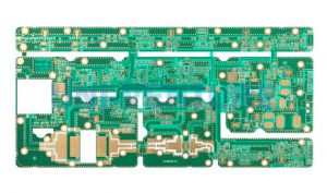
RF Via Structures and Why Are They Important in RF PCBs?
Trace width and spacing become extremely important at higher frequencies to maintain controlled impedance. The width of the traces should be precisely measured and designed using specialized design tools to meet the characteristic impedance specifications. Also, the length of the traces should be kept as short as possible to minimize attenuation and loss. Finally, the layout should never place a RF trace and a normal trace parallel to each other. This can cause interference between the two traces and significantly decrease signal integrity.
Via size is an important aspect of RF PCB design because the diameter of the via determines its parasitic inductance. Using small vias can reduce the inductance and improve signal integrity. The via’s aspect ratio is also important, as a higher aspect ratio can increase the parasitic inductance and negatively impact performance.
For RF PCBs, it’s critical to use a plasma etch technology to ensure quality and consistency in the through-hole vias. This form of etching allows for a tight front-to-back registration and minimal tolerance for the via hole. In addition, a laser direct imaging (LDI) process can provide accurate surface registration and maintain a consistent via depth. This is especially useful in RF PCBs, where precision is essential for maintaining the desired characteristic impedance of a signal.